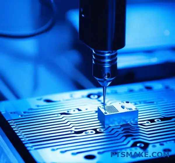
Semiconductor manufacturers face a harsh reality: a single micron-level tolerance error can destroy entire production batches and cost thousands in rework. Traditional machining methods often fall short when creating the ultra-precise components that modern semiconductor equipment demands, leaving engineers scrambling for reliable solutions.
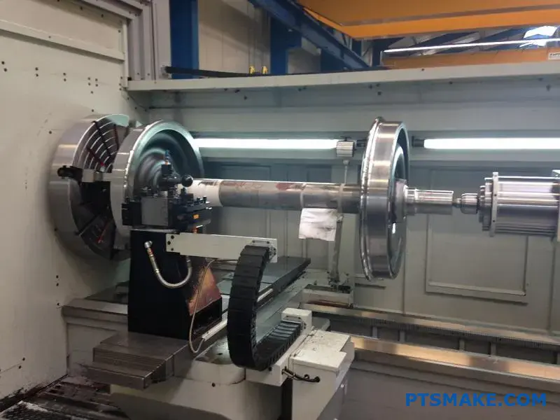
CNC machining provides semiconductor manufacturers with the precision, repeatability, and surface finish quality needed for critical components like housings, fixtures, and test equipment. This manufacturing method achieves tolerances as tight as ±0.0001 inches while maintaining consistent quality across production runs.
The semiconductor industry’s rapid evolution means you need manufacturing partners who understand both the technical challenges and business pressures you face. This guide breaks down everything from tolerance management and material selection to cost optimization and quality control strategies that successful semiconductor companies use to stay competitive.
Why Semiconductor Manufacturers Can’t Afford Tolerance Errors
In the world of semiconductor manufacturing, there is no room for "almost right." Precision is everything. Even a deviation measured in microns, smaller than a human hair, can cause catastrophic failures.
This isn’t just about quality control. It’s about the fundamental physics that make modern electronics possible. Tight semiconductor machining tolerances are not a luxury; they are a baseline requirement.
The Cost of Inaccuracy
Even a minor slip in precision has huge costs. The impact goes beyond a single faulty component.
| Tolerance Error | Consequence | Financial Impact |
|---|---|---|
| 1-2 Microns | Signal Integrity Loss | Moderate |
| 3-5 Microns | Overheating/Shorts | High |
| 5+ Microns | Complete Chip Failure | Critical |
Effective CNC precision for semiconductor parts is the only way to prevent these issues.
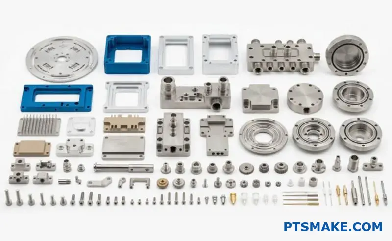
The demands for smaller, faster, and more powerful chips push manufacturing limits. This directly translates to stricter requirements for every single component. At PTSMAKE, we see this every day. Our clients need high-tolerance CNC parts that perform perfectly.
The Ripple Effect of a Single Error
A small tolerance error in one component doesn’t stay small. It creates a chain reaction. A slightly misaligned heatsink, for example, can lead to thermal management failure. This failure can then cause the entire chip to underperform or burn out completely. This is why every step, from material selection to the final cut, must be controlled. Factors like tool wear, vibration, and even slight temperature changes can affect the final product.
Based on our tests, a consistent environment is critical for repeatable accuracy. This environment control helps manage issues like thermal expansion1.
From Component to System Failure
Understanding the chain reaction is key. A single faulty part impacts the whole system.
| Component Defect | Sub-system Impact | Final Product Failure |
|---|---|---|
| Misaligned Contact Pin | Faulty Electrical Connection | Intermittent Device Operation |
| Poor Surface Finish | Inefficient Heat Transfer | Overheating and Shutdown |
| Incorrect Diameter | Seal or Gasket Failure | Contamination of Wafer |
This is why we focus so heavily on process control for every semiconductor cnc machining project we undertake.
In semiconductor manufacturing, precision is not a feature but a foundational necessity. Even micron-level tolerance errors can cascade into significant performance failures and financial losses, making strict control over high-tolerance CNC parts absolutely essential.
The Complete Cost-Benefit Analysis Of CNC Machining For Semiconductor Parts
Understanding the true cost of semiconductor CNC machining requires looking beyond the final price tag. It’s a balance of several key factors. Each stage, from initial design to full production, has its own economic impact.
Breaking Down Core Cost Components
Let’s dissect the primary cost drivers. Prototyping costs are upfront but crucial for validation. Material selection also heavily influences the budget, especially with expensive, high-purity materials required for semiconductor parts.
Tooling and Setup
Tooling for CNC is often less expensive than for methods like die casting. This is especially true for complex geometries. Setup time is a factor, but it offers flexibility for design changes.
Production Volume
The economics change with scale. CNC is highly cost-effective for low-to-mid volumes. High-volume runs may favor other methods, but often at the cost of precision.
Here is a quick overview of cost factors:
| Cost Component | CNC Machining Impact | Notes |
|---|---|---|
| Prototyping | Moderate to High | Fast turnaround, design flexibility |
| Material Waste | Moderate | Subtractive process, but optimizable |
| Tooling | Low to Moderate | No hard tooling needed |
| Production | Best for low-to-mid volume | Per-unit cost is stable |
When evaluating the total cost, we must compare semiconductor CNC machining against other viable manufacturing methods. Each technique has its own economic profile, making the choice dependent on your project’s specific needs. It’s about finding the sweet spot for your application.
CNC Machining vs. Alternative Methods
Methods like die casting or stamping are common in manufacturing. However, they often fall short for semiconductor applications. The tight tolerances and complex features required are where CNC shines. Die casting involves high initial mold costs. This makes it unsuitable for prototyping or small production runs. Stamping is great for simple, high-volume metal parts. Yet, it lacks the ability to create the intricate 3D geometries often found in semiconductor components. This process is a classic example of subtractive manufacturing2, where precision is paramount.
A Comparative Look
Based on our analysis with clients, the choice becomes clear when you map process capabilities to project requirements. For high-precision parts needing exotic materials, the semiconductor machining economics favor CNC. It avoids the massive upfront tooling investment of alternatives. This makes it a cost-effective CNC machining solution.
| Method | Best For | Tooling Cost | Precision | Material Choice |
|---|---|---|---|---|
| CNC Machining | Prototypes, Low-Mid Volume | Low | Very High | Wide |
| Die Casting | High Volume | Very High | Moderate | Limited (Metals) |
| Stamping | Very High Volume (Simple) | High | Low | Limited (Sheet Metal) |
Understanding the cost components and comparing manufacturing methods is key. CNC machining offers unparalleled precision and flexibility for semiconductor parts, especially for prototyping and low-to-mid volume production. It balances initial costs with final part quality and performance effectively.
Secrets To Achieving Ultra-Fine Surface Finish In Semiconductor Housings
Achieving an ultra-fine finish is not about one secret trick. It’s about precise control over the entire process. The right machine settings are fundamental.
For a superior surface finish CNC semiconductor component, we meticulously balance key parameters. This balance is critical for the final outcome.
Key Machine Settings
We start by optimizing spindle speed and feed rate. High spindle speeds with a controlled, slower feed rate often yield smoother surfaces. Tool selection and sharpness are equally important.
| Setting | Impact on Finish | General Recommendation |
|---|---|---|
| Spindle Speed | Higher speeds can reduce tool marks. | Maximize based on material and tool. |
| Feed Rate | Slower rates create a smoother path. | Minimize without causing tool rub. |
| Depth of Cut | Lighter finishing passes prevent stress. | Use a very shallow final pass. |
These adjustments are the first step toward achieving a low Ra value CNC machining result.
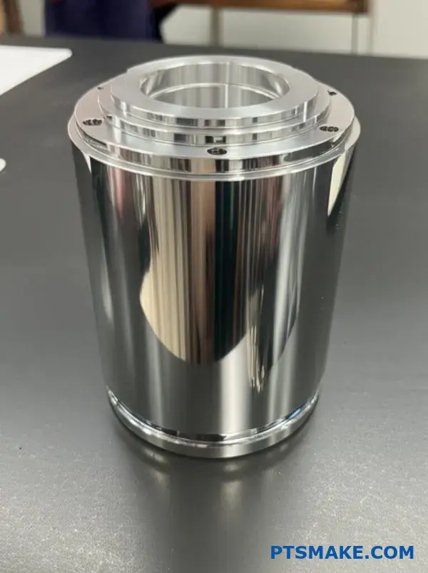
While machine settings lay the groundwork, material choice and post-processing elevate the finish to the next level for demanding semiconductor cnc machining applications. Not all materials are created equal when it comes to achieving a mirror-like surface.
The Crucial Role of Material
Certain aluminum alloys, like 6061-T6, are excellent for machining. They respond well to fine-tuning and polishing. Other materials might be harder or more brittle. This makes achieving a low Ra value3 more challenging without specialized techniques. Our approach at PTSMAKE always starts with a material analysis. This ensures the best possible foundation for a superior finish.
Refining the Surface with Polishing
After machining, we often use post-processing to reach the lowest Ra values. Techniques like CNC lapping and polishing are essential. These processes use abrasive slurries to methodically remove microscopic peaks from the material’s surface. This creates an exceptionally smooth and often reflective finish, which is critical for many semiconductor applications.
| Post-Processing Method | Best For | Typical Result |
|---|---|---|
| CNC Lapping | Achieving extreme flatness | Sub-0.1 µm Ra |
| Mechanical Polishing | Cosmetic and functional smoothness | < 0.2 µm Ra |
| Electropolishing | Complex geometries, stress relief | < 0.4 µm Ra |
Achieving an ultra-fine surface finish depends on a three-part strategy. It starts with precise CNC machine settings, is supported by proper material selection, and is perfected with post-processing techniques like CNC lapping and polishing for the final result.
Avoid These Material Pitfalls In Semiconductor CNC Projects
Choosing the right material for semiconductor components is crucial. A wrong choice can lead to project failure. It impacts performance, cost, and lead times.
Many projects rely on common materials. But they often overlook the hidden risks. Understanding these pitfalls is key to successful semiconductor CNC machining.
Common Material Challenges
Here’s a quick look at some popular CNC materials for semiconductors. Each has unique advantages but also significant machining risks.
| Material | Key Advantage | Common Pitfall |
|---|---|---|
| Ceramics | Extreme Hardness | Brittleness & Cracking |
| Titanium | Strength-to-Weight | Poor Heat Dissipation |
| Aluminum | Cost-Effective | Galling & Tool Buildup |
These issues can compromise the integrity of high-precision parts.
Material selection involves a trade-off. It’s about balancing final application needs with manufacturability. At PTSMAKE, we guide our partners through this process. We help avoid costly mistakes before they happen.
The Ceramic Conundrum
Advanced ceramics are incredibly hard and heat-resistant. This makes them ideal for certain semiconductor applications. However, their brittleness presents a huge machining challenge. Minor vibrations or improper tool pressure can cause catastrophic fractures. Machining them requires specialized tools and expertise.
Aluminum vs Titanium in Chips Hardware
Titanium offers excellent strength and corrosion resistance. But it has poor thermal conductivity. Heat builds up at the cutting edge, causing rapid tool wear. This can also cause work hardening4, making the material even tougher to cut.
Aluminum is much easier on tools and machines faster. But its softness can cause material to weld to the tool. Its high thermal expansion also demands careful management. This is vital to maintain tight tolerances during the machining process.
The machinability of semiconductor materials is a critical factor.
| Challenge | Titanium | Aluminum | Ceramic |
|---|---|---|---|
| Tool Wear | High | Low | Very High |
| Heat Mgmt | Difficult | Easy | Moderate |
| Brittleness Risk | Low | Low | High |
| Thermal Expansion | Low | High | Very Low |
Selecting the right material requires understanding these deep process challenges.
Successful semiconductor CNC machining demands a focus on manufacturability, not just material properties. Overlooking risks with ceramics, titanium, or aluminum can derail your project. A strategic approach considering both aspects ensures quality, cost-effectiveness, and reliability for critical components.
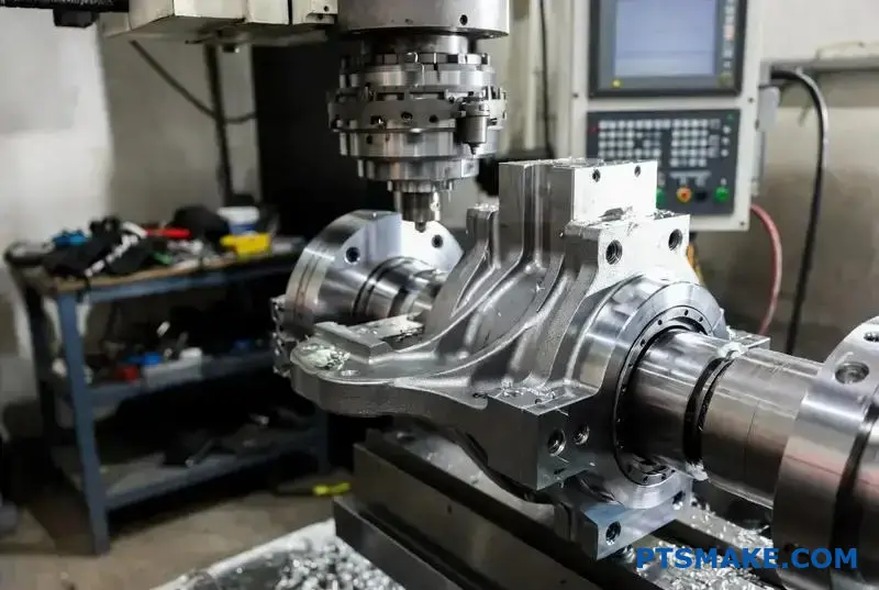
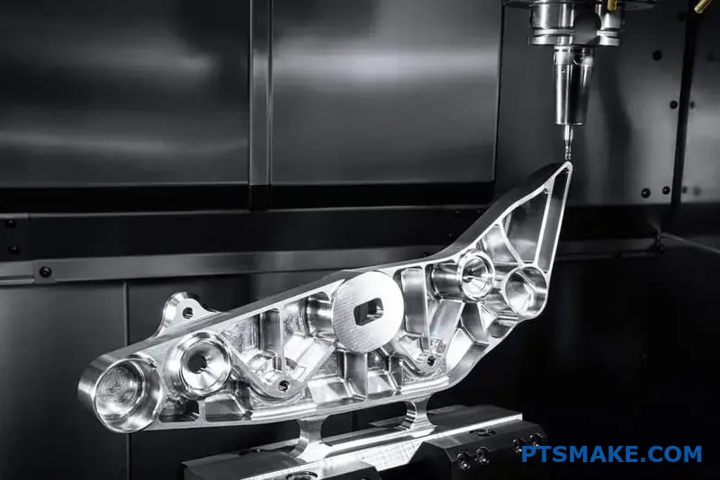
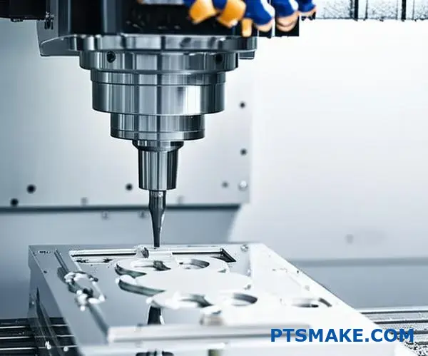
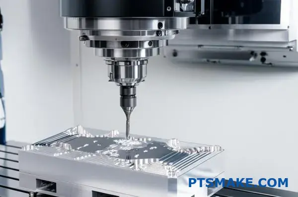
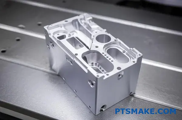
Why 5-Axis Is A Game-Changer For Semiconductor Components
Modern semiconductor parts are incredibly complex. They feature intricate channels, deep pockets, and angled surfaces. Standard 3-axis machines struggle with these.
This is where 5-axis CNC machining becomes essential. It allows the cutting tool to approach the workpiece from five different directions in a single setup. This capability is not just an upgrade; it’s a necessity for creating today’s high-precision semiconductor hardware.
Unlocking Complex Geometries
5-axis machining directly enables the creation of features that are otherwise impossible. It provides superior access to all faces of a part.
| Axis Capability | Tool Access | Suitable For |
|---|---|---|
| 3-Axis | Limited (Top-down) | Simple, flat components |
| 5-Axis | Multi-directional | Complex, multi-featured parts |
This improved access means we can machine intricate cooling channels or undercuts without repositioning the part. It’s a fundamental shift in manufacturing efficiency.
The single most significant advantage of 5-axis machining is the reduction in setups. With a 3-axis machine, a complex part might need to be manually re-fixtured multiple times. Each setup introduces a small risk of error.
These errors accumulate, a problem known as tolerance stack-up. For semiconductor components where microns matter, this is unacceptable. By completing a part in one or two setups, 5-axis machining drastically improves accuracy. Our internal studies at PTSMAKE show this can improve dimensional consistency by up to 40% on certain parts.
Superior Surface Finish and Tool Life
Continuous 5-axis toolpaths allow the cutting tool to maintain an optimal angle against the material. This avoids the "stop-and-go" motion of 3-axis machining. The result is a smoother surface finish, eliminating the need for secondary polishing processes.
This constant engagement also reduces chatter and wear on the tool. This prevents tiny imperfections caused by Tool Deflection5, which is critical for flawless high-precision semiconductor hardware.
| Machining Aspect | 3-Axis CNC | 5-Axis CNC |
|---|---|---|
| Setups Required | Multiple | Single / Fewer |
| Positional Accuracy | Lower | Higher |
| Surface Finish | Stepped / Rougher | Smoother / Continuous |
| Cycle Time | Longer | Shorter |
Ultimately, this advanced control over tool orientation and movement makes complex geometry machining not just possible, but also reliable and repeatable.
5-axis CNC machining revolutionizes the production of complex semiconductor parts. It ensures higher precision by minimizing setups, provides superior tool access for intricate designs, and achieves a better surface finish, making it an indispensable technology in the industry.
How To Reduce Lead Time With CNC Machining Without Sacrificing Quality
Shortening production cycles is key. It allows for faster innovation. But speed cannot sacrifice quality.
We use specific strategies to achieve this. These include concurrent engineering, optimized tooling, and quick changeovers.
These methods directly shorten the CNC lead time for semiconductors. They ensure fast delivery precision parts.
| Strategy | Primary Goal | Impact on Lead Time |
|---|---|---|
| Concurrent Engineering | Reduce redesigns | Significant |
| Optimized Tooling | Decrease machine cycle time | Moderate |
| Quick Changeovers | Minimize machine downtime | Moderate |
Deeper Dive into Production Cycle Strategies
To truly cut lead times, we must look at the entire process. It starts long before the machine turns on. Effective planning is crucial for quick-turn machining services.
The Power of Collaboration
Many delays come from design flaws found during manufacturing. This forces costly and time-consuming redesigns. We avoid this with a specific approach.
Adopting Concurrent Engineering6 is a game-changer. Our design and manufacturing engineers work together from the very beginning of a project. This ensures the design is optimized for manufacturing (DFM).
This is vital for industries requiring semiconductor cnc machining. Complex parts demand this level of early collaboration. It eliminates surprises later on.
Smart Tooling and Fast Setups
The right tools and efficient setups are critical. We don’t just use standard tools. We select or create tooling optimized for specific materials and geometries. This reduces machining time.
Quick changeovers are another focus. By preparing tooling and fixtures offline, we minimize the time a machine sits idle between jobs. This practice is essential for delivering fast delivery precision parts.
| Benefit | Concurrent Engineering | Optimized Tooling | Quick Changeovers |
|---|---|---|---|
| Reduces Rework | ✅ | ||
| Lowers Cycle Time | ✅ | ||
| Increases Machine Uptime | ✅ | ||
| Improves Part Quality | ✅ | ✅ |
At PTSMAKE, these strategies are part of our standard workflow. They allow us to provide reliable, fast-turnaround services.
Implementing concurrent engineering, optimizing tooling, and streamlining changeovers are proven tactics. They drastically shorten CNC lead times. These strategies are essential for delivering high-quality, fast delivery precision parts on schedule, especially in demanding sectors.
How Semiconductor Design Engineers Can Streamline DFM For CNC Parts
Applying Design for Manufacturing (DFM) principles is crucial. It directly impacts the cost, quality, and lead time of your CNC parts. For semiconductor components, precision is non-negotiable.
This requires specific design rules. I’ll share some core guidelines we follow at PTSMAKE to ensure success. These tips help bridge the gap between CAD models and flawless physical parts.
Wall Thickness and Spacing
Maintaining adequate wall thickness is fundamental. Thin walls can warp or break during machining. Proper spacing between features is also key for tool access.
| Material | Minimum Wall Thickness (Recommended) |
|---|---|
| Aluminum | 0.8 mm (0.031 in) |
| Stainless Steel | 1.0 mm (0.040 in) |
| Plastics (PEEK, etc.) | 1.5 mm (0.060 in) |
Feature Depth Optimization
Deep pockets and holes increase tool wear and machining time. A good rule of thumb is to keep pocket depths less than six times the tool’s diameter.
Mastering DFM for CNC goes beyond basic rules. It involves thinking like a machinist during the design phase. This perspective helps anticipate manufacturing challenges before they arise, especially in complex semiconductor applications.
CNC-Friendly CAD Practices
One of the best CNC-friendly CAD tips is standardizing features. Using standard drill sizes instead of custom ones significantly reduces setup time and cost. Always add radii to internal corners. Sharp internal corners require specialized, slower processes.
After analyzing results with our clients, we’ve found that material choice also plays a huge role. The properties of a material, such as its Anisotropy7, can affect how it behaves under the stress of machining. This influences the final part’s dimensional stability and performance.
Tool Access and Radii
Consider how a cutting tool will access each feature. Avoid deep, narrow channels. For internal corners, a larger radius is always better and cheaper to machine.
| Corner Radius | Machining Speed | Cost Impact |
|---|---|---|
| 0.5 mm | Slow | High |
| 1.0 mm | Medium | Moderate |
| >2.0 mm | Fast | Low |
Following DFM guidelines for CNC parts ensures smoother production. Optimizing wall thickness, feature depth, and using CNC-friendly CAD tips directly reduces manufacturing costs and improves part quality for semiconductor components. This proactive approach streamlines the entire process from design to delivery.
Insider’s Guide To Tighter Quality Control In Semiconductor CNC Production
In semiconductor manufacturing, saying a part is "correct" is not enough. You must prove it with data. This is where metrology and documentation become critical. They are the backbone of trust.
Key Metrology Techniques
We use specific tools for semiconductor part verification. Each tool has a distinct role in ensuring parts meet the highest quality standards for CNC machining. Precision is non-negotiable here.
| Tool | Primary Use |
|---|---|
| CMM | Verifying complex geometric dimensions |
| Digital Microscope | Inspecting surface finish and micro-features |
| SPC | Monitoring and controlling production processes |
This combination ensures every angle and surface meets exact specifications. It forms our core approach to precision quality control CNC.
Trust is built on verifiable proof. In semiconductor CNC machining, this proof comes from advanced measurement and exhaustive documentation. Without them, quality is just a guess.
Advanced Measurement and Verification
A Coordinate Measuring Machine (CMM) is essential. It measures a part’s geometry using a probe, providing precise data on complex features. Digital microscopy allows us to inspect surface finishes at a microscopic level, spotting imperfections invisible to the naked eye.
But measurement alone is reactive. We use Statistical Process Control8 to monitor production in real-time. This helps us predict and prevent deviations before they result in a failed part. It’s about proactive control.
Critical Documentation Flows
Documentation formalizes quality. It ensures everyone, from our engineers at PTSMAKE to your assembly team, is aligned. Each document serves a purpose in maintaining high quality standards for CNC machining.
| Document | Purpose |
|---|---|
| FAI (First Article Inspection) | Verifies the first production part against all specifications. |
| PPAP (Production Part Approval Process) | A comprehensive package proving the production process is stable. |
| ISO 9001 Certification | Demonstrates a commitment to a globally recognized quality management system. |
This rigorous documentation flow provides the transparency and accountability our clients in the semiconductor industry require. It’s not just paperwork; it’s our commitment to quality.
Advanced metrology tools provide precise data for semiconductor part verification. Rigorous documentation like FAI and PPAP, guided by ISO standards, ensures that precision is repeatable and verifiable, which is central to effective precision quality control CNC.
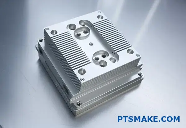
How To Mitigate Heat Build-Up Issues In CNC-Machined Semiconductor Fixtures
Effective thermal dissipation is critical. In test sockets and handling fixtures, heat can ruin test results. It can also shorten a component’s life.
Proper design is the first line of defense. This involves smart material choices and precise machining paths. Thermal control CNC machining ensures fixtures perform reliably under thermal stress.
We focus on creating thermal dissipation parts that are both effective and manufacturable. A well-designed fixture manages heat from the start.
Key Material Considerations
| Material | Thermal Conductivity | Best Use Case |
|---|---|---|
| Aluminum 6061 | High | General-purpose, good balance |
| Copper C110 | Very High | Maximum heat dissipation |
| PEEK | Low | Electrical insulation |
Deeper Dive into Thermal Management Strategies
Choosing the right material is just the beginning. The entire semiconductor cooling fixture design process must consider how heat moves through the part. This ensures reliable performance during intense testing cycles.
Material Selection Trade-Offs
While copper has superior thermal conductivity, it is heavier and more expensive than aluminum. For many applications, an aluminum alloy like 6061 offers a great balance of performance and cost. For parts needing insulation, we often turn to plastics like PEEK or Torlon. Some advanced composites even exhibit Anisotropic9 properties. This requires careful design consideration.
Machining Paths and Surface Finish
The toolpaths used in semiconductor cnc machining directly impact thermal performance. We machine specific textures or channels to guide heat flow. A smoother surface finish also ensures better contact with a device or an external heat sink, improving thermal transfer.
Integrated Heat Sinks
We often design fixtures with integrated heat sinks. CNC machining allows us to create complex fins and features. These features dramatically increase the surface area for heat dissipation. This is far more effective than a simple, flat block of material. Our tests show this can improve cooling by over 30%.
| Strategy | Primary Benefit | Implementation Detail |
|---|---|---|
| Material Choice | Optimizes conductivity/cost | Match material to thermal load |
| Machining Path | Enhances heat transfer | Create smooth surfaces or channels |
| Integrated Sinks | Maximizes surface area | Machine fins directly into the fixture |
Effective thermal management in semiconductor fixtures combines material science with smart design. By carefully selecting materials, planning machining paths, and integrating cooling features, we create reliable, high-performance components that prevent heat build-up.
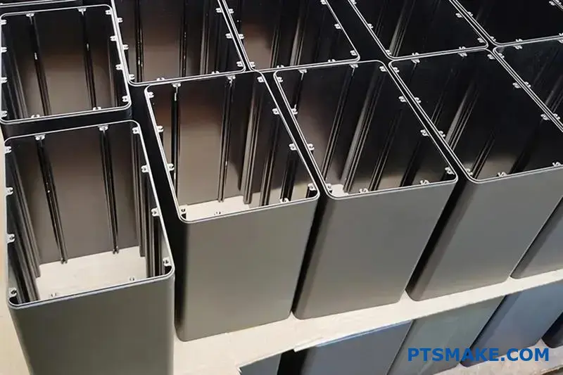
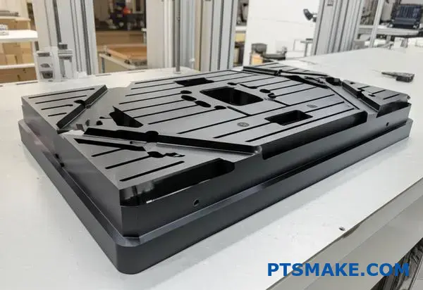
How To Handle Custom Semiconductor Enclosures With Extreme Geometry
Extreme geometry in semiconductor parts is no longer a barrier. Modern designs often require features that seem impossible to produce. Think of deep undercuts, complex internal cavities, or incredibly thin walls.
This is where CNC machining becomes the essential solution. It offers precision and control that other methods can’t match. For custom CNC enclosures, this capability is critical. It transforms radical concepts into functional, high-performance components.
The CNC Machining Advantage
CNC provides direct solutions for challenging designs.
| Feature Challenge | CNC Machining Solution |
|---|---|
| Undercuts | Multi-axis toolpaths |
| Internal Cavities | Specialized long-reach tooling |
| Thin Walls | High-speed, low-force cutting |
This process makes complex parts CNC machining a reliable reality. It ensures every detail meets exact specifications.
Precision is everything in semiconductor housing machining. Complex designs are not just for looks; they are for function. They manage heat, shield from interference, and fit into tight spaces. CNC machining directly addresses these needs.
Mastering Complex Geometries
At PTSMAKE, we handle these challenges daily. Multi-axis CNC machines are key. They allow the cutting tool to approach the workpiece from many different angles.
Undercuts and Internal Cavities
Creating undercuts and internal shapes is straightforward with 5-axis machining. The machine tool can tilt and rotate. This eliminates the need for multiple setups, which saves time and reduces the risk of errors. A precise toolpath10 is programmed to navigate these complex internal features perfectly.
Achieving Thin, Rigid Walls
Thin walls require a delicate balance. You need strength without bulk. Our approach combines advanced material knowledge with optimized cutting strategies. We use high-speed milling with very sharp tools. This minimizes cutting forces and prevents the thin walls from deforming during the process.
Here’s how we tackle these issues:
| Geometric Challenge | Key CNC Strategy | Resulting Benefit |
|---|---|---|
| Complex Internal Channels | 5-Axis Simultaneous Machining | Uninterrupted internal fluid or air flow. |
| Walls <0.5mm Thick | High-Speed Finishing Passes | Maintained structural integrity, no warping. |
| Deep Pockets with Sharp Corners | Long-Reach & Custom Tooling | Perfect fit for internal components. |
This detailed control ensures every feature, no matter how small or complex, is produced exactly as designed.
Advanced CNC machining is the definitive solution for semiconductor enclosures with extreme geometries. It enables the creation of undercuts, internal cavities, and thin walls with high precision, turning complex designs into reality without compromising on quality or functional requirements.
How To Validate Dimensional Accuracy In CNC Semiconductor Parts Before Assembly
In semiconductor manufacturing, assembly is a high-cost, high-stakes process. A single part out of spec can cause catastrophic failure.
Therefore, validating dimensional accuracy before assembly is not just a quality step; it’s a critical risk-management strategy.
Why Pre-Assembly Checks Matter
Verifying tolerances in critical dimensions ensures that every component fits perfectly. This prevents expensive rework or scrap later on. It is the foundation of reliable semiconductor device performance.
Key Validation Tools
We rely on advanced tools for this. Coordinate Measuring Machines (CMM) and strict GD&T practices are essential. They provide the data needed for a successful CNC dimensional check on semiconductor parts.
A Closer Look at Verification Methods
Failing to catch a dimensional error before assembly can compromise an entire production run. The costs multiply quickly, not just in materials but also in lost time. At PTSMAKE, we’ve built our process around preventing these issues.
Using CMM for Ultimate Precision
A Coordinate Measuring Machine (CMM) is the gold standard for tolerance verification machining. It uses a highly sensitive probe to take precise 3D measurements of a part. This data is then compared directly against the original CAD model.
This process removes human error. It can detect deviations far smaller than what traditional tools can measure. It is essential for complex geometries found in semiconductor CNC machining.
The Language of GD&T
Drawings for semiconductor parts use a specific language to define tolerances. This system, known as Geometric Dimensioning and Tolerancing (GD&T)11, specifies not just size but also the form, orientation, and location of features. This ensures components interact exactly as designed, which is vital for assembly-fit precision machining.
| Verification Aspect | Traditional Calipers | CMM with GD&T |
|---|---|---|
| Measurement Scope | Basic length, width, diameter | Complex profiles, positions, flatness |
| Repeatability | Lower, operator dependent | High, fully automated |
| Data Analysis | Manual pass/fail checks | Detailed reports, statistical analysis |
| Application | Simple geometric checks | Critical semiconductor components |
Pre-assembly validation using CMMs and GD&T is fundamental. This rigorous CNC dimensional check for semiconductor parts ensures every component meets exact specifications, preventing costly assembly failures and guaranteeing final product integrity. It’s about precision, not chance.
When CNC Machining Beats Die Casting For Semiconductor-Grade Housings
Choosing the right manufacturing process is critical. Especially for semiconductor-grade housings. Die casting offers speed for high volumes. But it often falls short on precision.
This is where CNC machining excels. It provides the tight tolerances and superior surface finishes required.
Key Comparison Points
When you compare die cast vs CNC semiconductor parts, two factors stand out: tolerance and surface quality.
Tolerance Capabilities
Die casting struggles with consistency. Post-machining is almost always needed. CNC, however, starts with a solid block. It machines features to exact specifications from the start.
| Feature | Die Casting | CNC Machining |
|---|---|---|
| Typical Tolerance | ±0.05 mm | ±0.005 mm |
| Consistency | Lower | Higher |
| Post-Processing | Often required | Minimal |
This makes CNC ideal for semiconductor-grade parts CNC.
For parts where failure is not an option, precision is everything. The semiconductor industry demands near-perfect components. This is where the debate over manufacturing methods becomes most intense.
Why CNC Wins for Critical Surfaces
Die casting introduces risks. Issues like porosity, surface imperfections, and the need for draft angles can compromise a housing’s integrity. These are unacceptable for sensitive electronics. Trapped gases in die casting can create internal voids.
CNC machining avoids these problems entirely. We machine from a solid billet of material. This ensures structural integrity and uniform material properties. The process is free from the defects common in casting.
In precision housing manufacturing, material consistency is key. Working with clients, we found that machined parts exhibit more predictable thermal and mechanical behavior. This is crucial for performance. The material’s internal structure is not altered by melting and rapid cooling. This avoids issues like anisotropy12 that can affect performance under stress.
Use Cases Favoring CNC
CNC is the only logical choice for specific applications demanding the highest quality.
| Application | Key Requirement | Why CNC is Better |
|---|---|---|
| Vacuum Chamber Housings | Perfect Seal | No porosity, superior surface finish. |
| Optical Component Mounts | High Stability | Machined from a single block, no internal stress. |
| Heat Sinks | Flawless Surface Contact | Maximizes thermal transfer efficiency. |
These examples show where CNC provides unmatched value.
For semiconductor applications, the choice is clear. When tight tolerances and flawless surfaces are required, CNC machining consistently outperforms die casting, eliminating defects and ensuring the highest level of part quality and reliability for critical components.
Unlock Precision Results with PTSMAKE Semiconductor CNC Machining!
Ready to eliminate costly tolerance errors and accelerate your semiconductor innovation? Contact PTSMAKE now for a fast, accurate quote on high-precision CNC machining solutions. Let our expert team help you streamline production and guarantee your parts exceed every specification. Send your RFQ today!

Learn how temperature fluctuations can critically impact material dimensions and machining accuracy. ↩
Explore how this manufacturing approach delivers superior precision for intricate components. ↩
Understand how Ra is measured and why specific values are critical for semiconductor component performance. ↩
Discover how this effect hardens the material during machining, increasing difficulty and tool wear. ↩
Understand how tool bending impacts precision in complex geometry machining and how we mitigate it for superior results. ↩
Learn how this collaborative approach integrates design and manufacturing to accelerate your product development timeline. ↩
Understand how material grain direction can impact the precision and performance of your machined parts. ↩
Understand how SPC uses data to ensure consistent quality and process stability. ↩
Understand this concept to select advanced materials for complex thermal challenges. ↩
Understand how precise toolpath programming directly impacts your part’s final quality and cost. ↩
Click to learn the core principles of GD&T and why it is essential for modern manufacturing. ↩
Learn how directional material properties can impact the precision and stability of your machined components. ↩